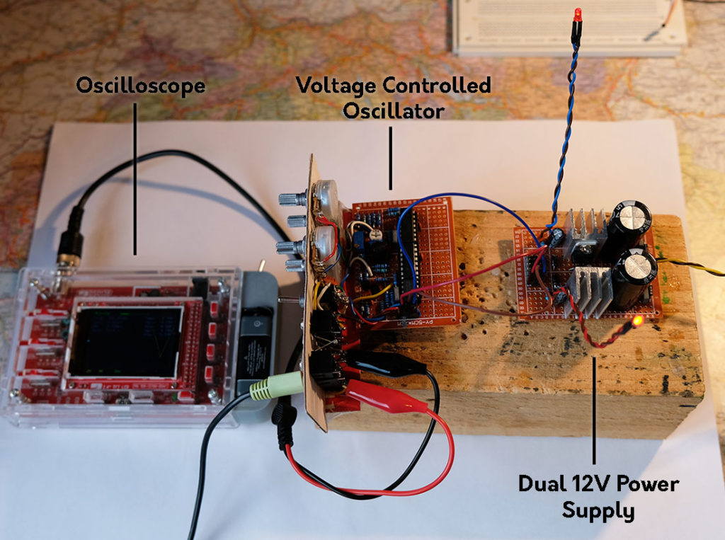
The very first thing which needs to be addressed when building a DIY synthesiser is how will it all be powered? Traditionally, synthesisers require both positive and negative voltages, which makes putting together a suitable power supply slightly trickier than it may at first seem. By convention, audio signals generated by an oscillator should have an amplitude of around 10V centred on ground (-5V at the lowest point, +5V at the highest). Therefore, the power supply needs to deliver voltages that are above ±5V. The most common supply voltages are ±9V (for battery operated systems), ±12V (for Eurorack modules) and ±15V. In this tutorial, I’ll discuss the three most common circuit designs used to provide power for modular synthesisers.
Note: Some of the circuits described in this post use mains power, and can be dangerous if built incorrectly. Since all other circuits in the synthesiser depend on a stable source of power, making a mistake in the power supply can cause a variety of issues to any connected modules. If you don’t have the experience or equipment to build your own power supply from scratch, I would encourage you to get a pre-assembled one or a circuit board kit instead!
1. Series Battery Method
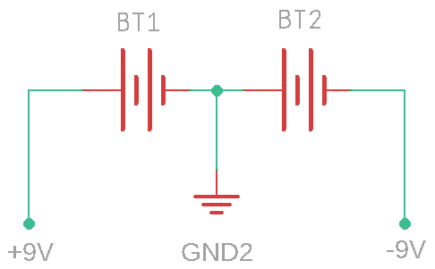
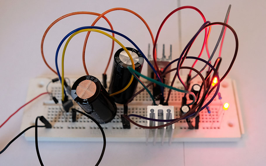
One of the simplest ways to create a dual power supply is by using two sets of batteries. The batteries are connected in series, so that the positive terminal of one battery is attached to the negative terminal of the second battery. When this middle connection is used as the ground reference for the circuit, you will be able to get a positive and negative voltage from the batteries, as shown in the circuit diagram below. For small and portable synthesisers, this is often done using two 9V batteries as I’ve demonstrated on a breadboard in the image below. Since the voltage of both batteries will drop as the power is drained, we also need to include voltage regulators which ensure a stable voltage is supplied to the synthesiser. In the image below, you can see that the batteries I am using are almost empty as the voltage measured by my multimeter is only -7.11V.
This method only works when one or both voltage sources are said to be “floating”. This means that the power source is not connected to any absolute reference voltage, such as a connection to Earth. All batteries are floating power sources, however wired power supplies often aren’t. For example, if the negative terminal of both voltage sources is connected to ground, then attaching the positive and negative terminals of both sources together will simply create a short-circuit; this is something I would encourage you to avoid!
- Benefits:
- Very easy to implement and troubleshoot.
- Relatively Portable.
- Voltage can be increased by adding more batteries in series.
- The battery life and maximum output current can be increased by adding more batteries in parallel.
- Disadvantages:
- Batteries constantly need to be replaced!
- The voltage of the batteries will drop as they run out (as seen in the image), so an additional power regulator IC will still be required.

2. Dual AC to DC Rectification
The electricity being supplied in the mains socket alternates from a positive to a negative voltage many times a second (230V 50Hz in Europe, 120V 60Hz in the US). What we want to do is reduce this voltage down to a lower and more manageable voltage, taking the positive half of the AC signal to supply the positive output and the negative half for the negative output. This process requires the following steps:
- Step down the high voltage being supplied by the mains to a lower voltage using a transformer.
- Rectify the AC signal into a positive and negative signal using diodes.
- Smooth out the voltage using capacitors.
- Generate a stable output voltage using power regulators.
a. Half-wave Rectifier Circuit
This is the power supply design I used in my synthesiser, and it is probably the most common design used by DIY synth builders. This design is often preferred to the Full-wave Rectifier as you can use a commercial wall plug transformer to convert the mains power down to 12V AC, which is used by the power supply. This means that your circuit does not directly come into contact with the mains power, making it a little bit safer to work with (but you still need to be careful!).
Important: You need to make sure that the wall plug transformer you use outputs 12V alternating current, and not 12V direct current. The 12V DC plugs are a lot more common, so it may take some searching to find the correct type of 12V AC plug. Also make sure that the plug you get is rated for a current of at least 1000mA or above, and that the mains voltage input rating is correct for the country you are in.
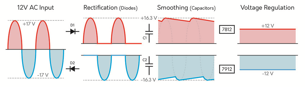
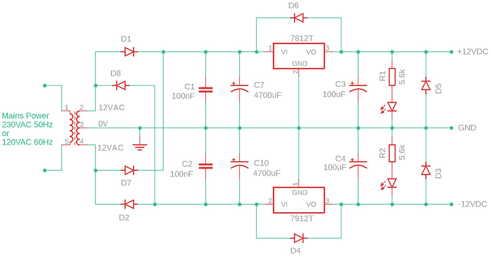
An example of a half-wave rectifier circuit is shown in Schematic 2 below. The circuit takes in a 12V AC signal from the wall plug, and converts it into a stable positive and negative 12V output. I have seen many variations of this circuit, using a wide variety of different capacitor values.

How does it work?
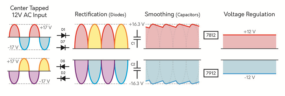
- The circuit takes in a 12V alternating current signal from the wall plug transformer. 12V AC refers to the root mean square (RMS) value of the signal. This signal has a peak voltage of ±17V, as shown in the waveform diagram below.
- The diode D1 only allows the positive half of the AC signal to pass through, while D2 lets negative voltages through. This process is known as half-wave or half-bridge rectification, since only half of the AC waveform is used to power each of the voltage outputs. As a result, each output can theoretically only output half of the power (and consequently current) delivered by the wall plug transformer. The peak voltage of the rectified signals is ±16.3V, since the diodes introduce a 0.7V drop into the circuit.
- The capacitors smooth out the waveform, ensuring that a more continuous voltage is being supplied to the voltage regulators. The reasoning behind selecting this specific capacitance value is discussed in the next section.
- The LM7812 and LM7912 voltage regulators ensure that the outputs of the power supply stay at a stable +12V and -12V respectively. If you want to get +15V and -15V outputs instead, you can use a 15V AC power plug and replace these with the LM7815 and LM7915 regulators. If you are putting together your own circuit, watch out as the input, output and ground pins are in a different order on the positive and negative voltage regulators.
- Capacitors C3 and C4 are mainly included to improve the transient response of the power supply; the capacitor can provide brief bursts of high current when there are sudden changes in load being applied to the power supply. According to the data-sheet for the negative voltage regulator LM7912, for stability the capacitor C4 should be at least 1μF (using a tantalum capacitor) or 10μF (using an electrolytic capacitor). The higher value of 100μF was chosen to give an additional factor of safety over this minimum value.
- The two LEDs are there to indicate that there is power at the outputs. Some negative power regulators also require a minimum load to be applied at the output before they start up, so the LEDs help to provide that load.
- According to the data-sheet for LM7912, the diode D4 is required when large capacitors such as C10 are used at the input. The diode prevents momentary input short circuits, which can occur when the circuit is powered up or down. The LM7812 does not necessarily need this, but I put D6 in for good measure.
- The data sheet for both LM7812 and LM7912 specify that D5 and D3 should be present to prevent latch-up problems. These components act as clamping diodes, helping to protect the regulators from reversed polarity on the outputs. If one regulator starts up before the other one, devices such as operational amplifiers (op amps) can latch up and cause a short circuit between both power rails. This can prevent the second regulator from starting up. The diodes (preferably Schottkey) prevent the positive output from going below -0.3V and the negative output going above 0.3V, allowing both regulators to start up and the latch up condition to stop.
How to choose the capacitor values?
Why are there two capacitors at the input of each power rail (C1 & C7, C2 & C10)? How were the values of these capacitors chosen? I’ve looked at several schematics for half-wave rectifiers and there seems to be a lot of variance in what the capacitance value should be.
Generally there is one small non-electrolytic capacitor close to the input of each power regulator, which helps to stabilise, filter and smooth the input (C1 and C2). Usually this is between 100nF to 1μF. Small capacitors (ceramic, polyester, tantalum etc.) tend to be better than larger electrolytic film capacitor at filtering out high-frequency noise from the signal.
Then there is a bank of large electrolytic capacitors connected in parallel (C7 and C10; more capacitors can be connected if required), ensuring that there is a relatively constant reservoir of power even when the AC input signal is in the opposite half of the wave and no new power is being supplied. These capacitors are good at removing low frequency noise and stabilising variances in the DC voltage. The total capacitance of this reservoir depends on the amount of load you expect to put on the power supply. Here is how to calculate how much capacitance you may need:
According to the datasheet, the 12V regulators need a minimum input voltage of 14.5V to be able to provide a stable 12V output. Since 16.3V is the maximum voltage provided by our transformer and rectification circuit, under full load we are aiming for an average DC input voltage (VDC) of 15.4V and maximum voltage ripple (p%) of 5.8%.
V_{DC}=\frac{16.3+14.5}{2}=15.4V\rho_\%=\frac{15.4-14.5}{15.4}\times100=5.8\%Next we need to calculate the effective resistance of the load. Since the regulator can output a maximum current (IDC) of around 1A, this means that the equivalent load resistance (RL) is 15.4 ohms. The power dissipated (PD) across the regulator (in the form of heat) is 3.4W. The regulator can only dissipate ~1W on its own, so we definitely need to attach a heatsink to it to remove the excess heat.
R_L=\frac{V_{DC}}{I_{DC}}=\frac{15.4}{1}=15.4\OmegaP_D = (V_{DC}-V_O )(I_{DC})\newline=(15.4-12)(1)=3.4WWe can then calculate a minimum capacitance value (Cs) which can provide the desired voltage ripple. The formula I am using assumes that the capacitor discharge is approximately linear and that the AC frequency is 50Hz. The value turns out to be around 11,000µF! We theoretically would need to connect 3 of the large 4700µF capacitors together in parallel so that the power regulator could reach its maximum output current of 1A. With only one 4700µF capacitor the maximum output current is probably around 0.4A per rail.
C_s=\frac{1}{\rho _\%R_L}=\frac{1}{5.8\times 15.4}=0.011F\text{If } \quad C_s=0.0047F \quad \text{then:}R_L=\frac{1}{5.8\times 0.0047}=36.7\OmegaI_{DC}=\frac{15.4}{36.7}=0.42ASo to summarise… if we want to get a full 1A of output current from our power supply, the combined capacitance value at the input of the regulator needs to be at least 11,000µF.
Half-bridge Rectifier: Further Reading
- Music from Outer Space: Wall-wart Power Supply
- Circuits Today: Half-wave Rectifier Circuit Theory
b. Full-wave Rectifier Circuit
In a “full-bridge” or “full-wave” rectification circuit, both the positive and negative sections of the alternating waveform are used to power both outputs. This means that the circuit can theoretically drive twice the load compared to a half-bridge rectifier. As can be seen in Schematic 3, most of the circuit is identical to the half-bridge rectifier. The only differences are that two additional rectification diodes have been added, and a transformer with three outputs (called a “Center Tapped Transformer”) is used. The central output of the transformer is used as the ground reference, while the other two connections output an identical 12V AC signal, but out of phase by 180°. This means that when one of the outputs is in the positive section of the alternating waveform, the other is in the negative section and vice versa.
This type of circuit is often used in professional equipment, but is not used as much by DIY synthesiser builders. Center-tapped transformers are not available as a pre-packaged wall-plug, so you would need to wire your own. Since one end of the transformer is connected to mains power, building this circuit involves a bit more risk and should only be attempted if you have the right equipment and know what you are doing! When buying a transformer, make sure that the mains voltage input rating is correct for the country you are in.
How does it work?
- The transformer takes the mains alternating signal and reduces the voltage, outputing two 12V alternating current signals which are out of phase by 180°.
- The four diodes are used to separate the positive and negative sections of the alternating signal, directing the positive halves to the +12V regulator and the negative halves to the -12V regulator. Since both AC signals are out of phase, this results in a continuous supply of power for both polarities.
- The rest of the circuit is identical to the “half-bridge rectifier”, so you can refer to my description above to see how it works and what each component is doing.
Full-bridge Rectifier: Further Reading
- Circuit Digest: +-12V Dual Power Supply
- Circuits Today: Full Wave Rectifier-bridge Theory
- All About Circuits: Rectifier Circuits
3. DC to DC Inverting Charge Pump
It is also possible to generate a dual 12V power supply from only one +12V DC power plug. This is useful since DC power plugs are a lot more common and therefore cheaper to buy. It is also easier to find 12V DC plugs which have a high current rating, allowing more synthesiser modules to be powered from the same supply. This type of power supply design is often seen in portable modular synthesiser kits, and small Eurorack-compatible power modules. Since the transformer and rectification circuitry (large capacitors) are all contained within the external plug, the footprint of the electronics used in this design can be made a lot smaller than in the Dual AC-DC rectification circuits.
a. How does it work?
In its most simple form, an inverting charge pump uses a “floating” capacitor to carry charge over from the +12V side to the -12V side of the circuit. The capacitor is charged up from the +12V input being provided by the wall plug. Once full, the capacitor is disconnected from +12V input and the positive lead is instead connected to ground. Since the charge (and therefore voltage drop) across the capacitor remains the same, this means the negative terminal of the capacitor is now at a voltage of -12V. The capacitor then begins to discharge and this is used to power the negative rail. In our power supply, this process of charging and discharging is repeated many times a second. Schematic 4 shows an equivalent circuit, demonstrating how this system works. In a real circuit, the switching of the capacitor is done using an IC chip.
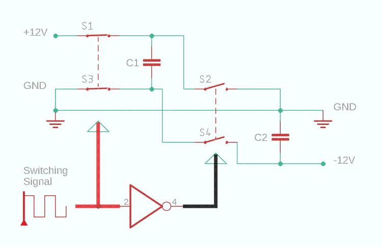
- Initially, switches S1 and S3 are closed while switches S2 and S4 are open. Capacitor C1 is connected to Vin and ground, causing the charge in the capacitor to increase.
- After a certain interval, the switches S1 and S3 are opened up again while S2 and S4 are closed. The top leg of the capacitor is now connected to ground instead of Vin. Since the charge in the capacitor hasn’t changed, there is still the same voltage drop across the capacitor. As a result, a voltage of -Vin is present on the bottom leg of the capacitor.
- This switching mechanism is continuously repeated, charging the capacitor C1 with the positive input voltage and de-charging it again on the inverted output. The capacitor is essentially pumping the charge from the positive input to the inverted output.
- Capacitor C2 acts as a power buffer/storage, smoothing the voltage on the output and ensuring that a continuous supply is available at the inverted output.
b. Implementing it in practice
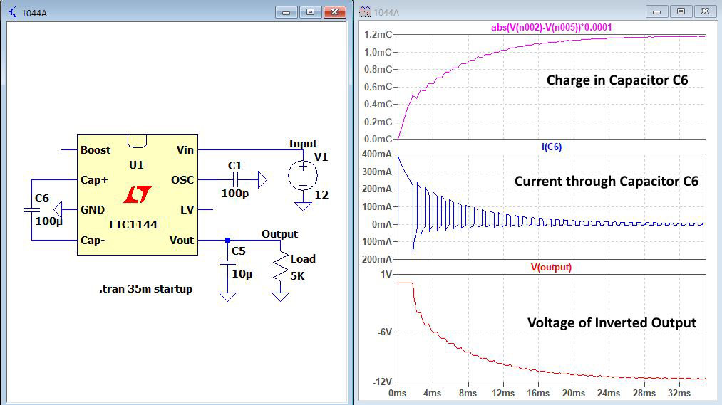
In the example circuit show in Schematic 5, we are using the LTC1144 chip made by Analog Devices to do the switching for out inverting charge pump. The capacitor C6 is used to invert the charge, while C5 acts as reservoir so that the negative output has a more stable output. The graphs show how the circuit reacts when it is started up. The current through the capacitor C6 alternates from positive to negative at regular intervals as it charges from the positive supply and de-charges into the negative output. The voltage of the negative output quickly decreases as the reservoir capacitor C5 is charged up, levelling out at -12V over time.
In the LTC1144 chip, the frequency of the switching signal can be increased or decreased by changing the value of the capacitor connected to the OSC input pin. Charge pumps can operate at a wide range of switching frequencies, usually ranging from 1kHz to as high as 200kHz.
Note: I haven’t had the chance to try this circuit out in practice, so the capacitor values in Schematic 5 will probably need to be altered to make it suitable for use as a synthesiser power supply. The circuit simulations were done in the free program “LTspice” made by Analog Devices.
Charge Pumps: Further Reading
- All About Circuits: Boosting and Inverting using a charge pump
- Maxim Integrated: In-depth tutorial of charge pumps
- EDN: The ins and outs of charge-pump-converter ICs
If you have any questions or suggestions, please feel free to leave a comment below!